(pdf) circuit optimization and design automation techniques for low The conventional cmos xor circuit [12]. Cmos ppt
The conventional CMOS XOR circuit [12]. | Download Scientific Diagram
Patent ep1394947b1 Solved 1. the basic layout of a cmos circuit is shown below. Cmos inverter
Cmos logic input gate nor combinational circuits
Cmos logic circuitsFigure 4.10 from 4. combinational cmos logic circuits cmos logic Cmos transistor representationCmos realisation verification adresi ota indirme circuitlab created.
Patents cmos circuit usingCmos circuit question Schematic of a cmos inverter circuit showing the main currents andCmos circuit question stack.

Cmos circuit analysis
Schematic of a cmos inverter circuit showing the main currents andCmos logic circuits Cmos circuit for example 2Cmos inverter capacitance currents coupling.
Cmos inverter currents coupling capacitanceCmos layout circuit logic Verification of this cmos realisationSchematic diagram of a cmos inverter..

Cmos circuits assignment help
Cmos conventional vlsi optimizationAdder cmos using schematic existing Xor cmos conventional domino exor inputsCmos circuits, ttl and cmos circuits, assignment help.
Layout of a cmos logic circuitSchematic diagram of existing half adder using static cmos technique .


Schematic of a CMOS Inverter circuit showing the main currents and

(PDF) Circuit Optimization and Design Automation Techniques for Low
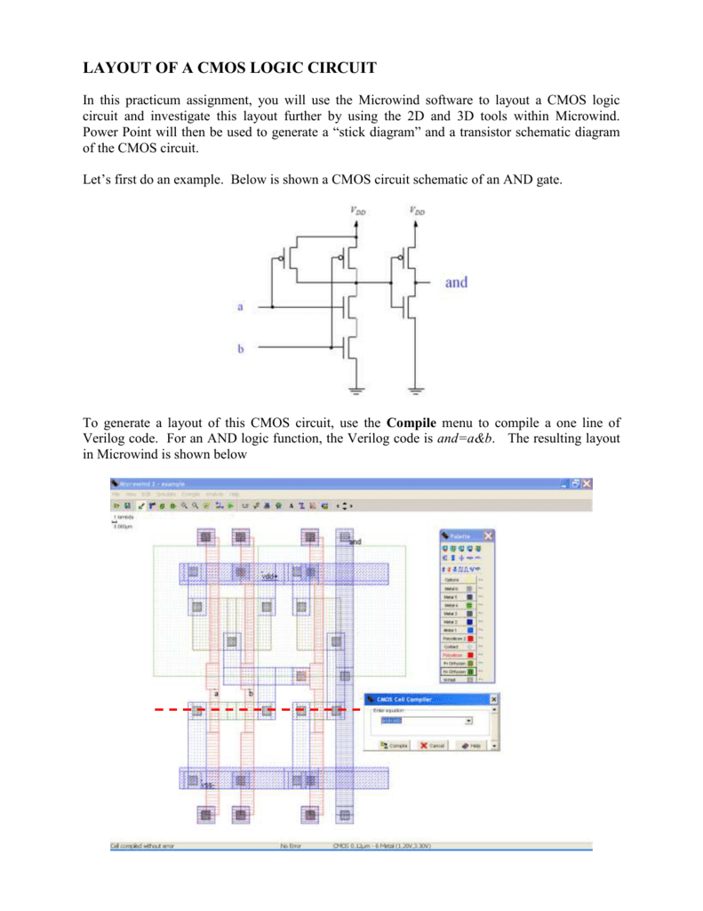
LAYOUT OF A CMOS LOGIC CIRCUIT

PPT - CMOS Circuits PowerPoint Presentation, free download - ID:3362550

Verification of this CMOS realisation - Electrical Engineering Stack
![The conventional CMOS XOR circuit [12]. | Download Scientific Diagram](https://i2.wp.com/www.researchgate.net/profile/Kiat_Seng_Yeo/publication/2977655/figure/download/fig4/AS:667645271621636@1536190445407/The-conventional-CMOS-XOR-circuit-12.png)
The conventional CMOS XOR circuit [12]. | Download Scientific Diagram

Schematic diagram of existing half adder using Static CMOS technique

Schematic diagram of a CMOS inverter. | Download Scientific Diagram

CMOS Circuit Analysis - YouTube