Digital logic part 3 Flip rs clocked flop latch nand flops table truth circuit digital gates circuits logic master vlsi encyclopedia electronics types sequential Flip flop flops sr jk clocked circuits electronics rs imperial set master type basic state use slave test should when
Solved 5U. Complete the timing diagram shown below for a | Chegg.com
Digital logic part 3 Flip flop clocked logic gate nor Sr flip flop circuit 74hc00
Types of flip-flop circuits explained
Flop sr timing clocked signals logicFlip flop sr nor clocked rs diagram sequential flops circuits latch circuit logic gates digital electronics latches gated flipflop description Flop flip circuit sr 74hc00 jk circuits flops bc547 transistors morse ne555 oscillator timerFlip flops, r-s, j-k, d, t, master slave.
Sr flip-flop circuit diagram with nand gates: working & truth tableFlip flop sr circuit clocked ic diagram diy based project Flip flop diagram timing clockedNand flops circuitverse.

How to test clocked circuits
Clocked r-s flip-flop tutorialSolved 5u. complete the timing diagram shown below for a Flip flop clocked clock circuit shownFlip flop clocked sr clock latch tutorial flops level.
What is jk flip flop? circuit diagram & truth tableDiagram timing flop flip sr edge triggered negative time complete solved below inputs assume 5u shown table transcribed problem text Dee2034 chapter 4 flip flop for students partDiy – clocked sr flip flop.

Flip flop sr circuit nand gates truth table symbol diagram using working
Flip flop jk diagram circuit truth table rs figure inputs bistable shown belowFlip flop rs types jk circuits flops explained logic diagram flipflop clock pulse works output hub bright engineering allowed reach The clocked t flip-flop timing diagramSr flip-flop circuit diagram with nand gates: working & truth table.
Flop clocked schematic logicClocked s-r flip-flop » examradar Flop flip nand sr circuit gates using gate diagram table truth which working circuits constructing below.


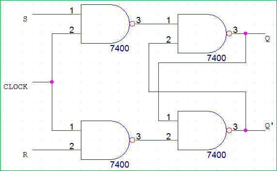
CircuitVerse - Flip-Flops using NAND Gate

Digital Logic Part 3 - Clock Signals

Solved 5U. Complete the timing diagram shown below for a | Chegg.com

SR Flip Flop Circuit 74HC00 - Truth Table

Digital Logic Part 3 - Clock SignalsRheingold Heavy

flipflop - sequential circuits; clocked SR flip-flop - Electrical

Flip Flops, R-S, J-K, D, T, Master Slave | D&E notes

Clocked S-R Flip-Flop » ExamRadar
SR Flip-Flop Circuit Diagram with NAND Gates: Working & Truth Table